Need something else?
Click here to tell us your requirements
Sapphire (Al₂O₃) Material Properties
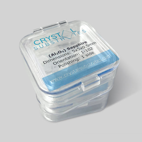
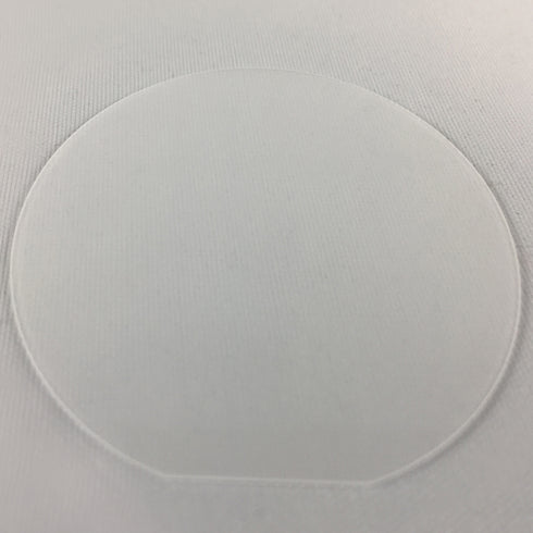
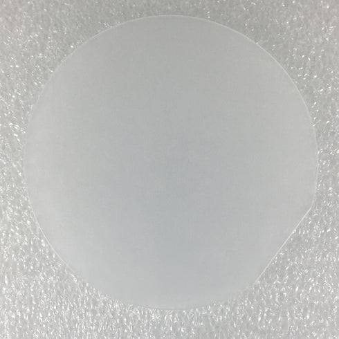
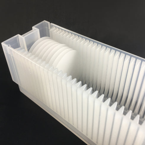
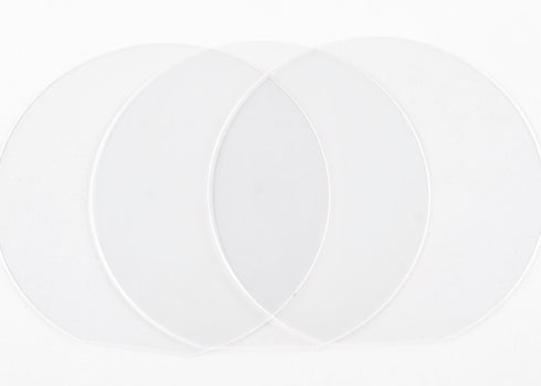
We offer a wide range of Al₂O₃ substrate sizes beyond those listed above, from 5x5mm to 4-6 inch (largest Al₂O₃ size depending on orientation).
Single crystal sapphire Al₂O₃ is chemically stable, electrically insulating, hard, temperature resistant and has high transparency in the UV-Visible wavelength range. It is easy to make in large crystals and due to its very high hardness it is possible to polish them to an atomically flat surface. As such it is a common choice for the growth of many thin films as well as other uses in and around the lab as a cheap, reliable flat surface.
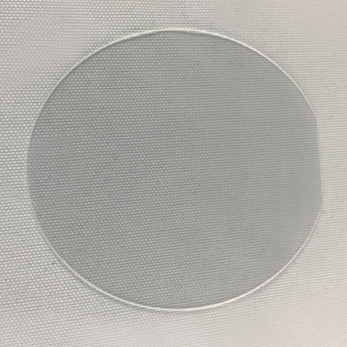
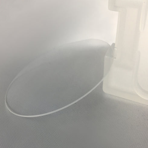
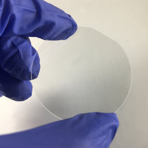
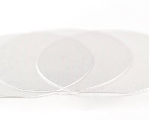
As Al₂O₃ is highly transparent (>85% in near UV-Visible-IR range 0.17 to 5.5 μm), it is commonly purchased double side polished so that you can perform transmission / absorption spectroscopy on thin films. But for any other use can be purchased single side polished.
Sapphire (α-Al₂O₃) as a hexagonal structure, belonging to the space group R3c, can be expressed both as a hexagonal (4 indices hkil) or as a rhombohedral unit cell (hkl). The Al atoms are octahedrally coordinated by six oxygen atoms. The oxygen ions nearly form a hexagonal close-packed structure with aluminium ions (Al3+) filling two-thirds of the octahedral interstices. Each Al3+ center is octahedral.
Sapphire (Al₂O₃) Planes
The figure below shows the common planes of Sapphire and those available from Crystal Substrates. C-Plane and A-plane are the most commonly used in the lab, but each have their use for stabilizing growth of specific orientations of thin film materials.

- C-plane : The most common orientation used for epitaxial growth of GaN in LED manufacturing, offering a hexagonal surface that aligns well with wurtzite-structured materials.
- A-plane : Provides an orthogonal surface to the c-axis, often used in optoelectronics and photonics for its unique anisotropic properties and lower thermal expansion mismatch with certain materials.
- R-plane : Features a rhombohedral surface, commonly employed in the growth of silicon carbide (SiC) and for applications requiring unique birefringent properties.
- M-plane : Used in the fabrication of non-polar and semi-polar GaN devices, offering a reduced electric field effect in optoelectronic applications, which can improve performance in LEDs and lasers.
- M-plane : A specific orientation within the M-plane family, utilized in applications requiring particular crystal orientations for specialized optical and electronic properties.
Commonly grown materials on sapphire (Al₂O₃) substrates:
ZnO, β-Ga2O3, AlN, GaN, CuGaO2, TiO2, LiCoO2, Spinel battery materials.
There is too much information out there on sapphire substrates and their uses to summarise here fully but if you have any questions, feel free to get in contact at info@crystal-substrates.com.
Dr Joseph Franklin
| LINEAR FORMULA: | |
| PURITY: | >99.99% |
| CRYSTAL ORIENTATION: | (100), (110) & (111) |
| GROWTH METHOD: | Czochralski |
| CRYSTAL STRUCTURE: | |
| LATTICE CONSTANT: | |
| MELTING POINT (°C): | 2040 C |
| THERMAL EXPANSION COEFFICIENT (/K): | 7.5 × 10⁻⁶ /°C |
| HARDNESS: | 9 |
| MOLAR MASS (G/MOL): | 101.96 g/mol |
| DENSITY (G/CM3): | 3.98g/cm3 |
| DIELECTRIC CONSTANTS: | |
| CHEMICAL STABILITY: | |
| SIZES: | 5x5mm & 10x10 mm |
| TYPICAL THICKNESS: | 0.5mm |
| SIZE TOLERANCES: | +/- 0.1mm |
| THICKNESS TOLERANCES: | +/- 0.015mm |
| ORIENTATION PRECISION: | +/-0.5 degree |
| POLISHING OPTIONS: | SINGLE SIDED (1SP) OR BOTH SIDES POLISHED (2SP) |
| ROUGHNESS RA: | <0.5nm |
| THERMAL CONDUCTIVITY | 46.06 @ 0 oC, 25.12 @ 100 oC, 12.56 @ 400 oC ( W/(m.K) ) |
| WATER ABSORPTION | 0% |
| FLEXURAL STRENGTH | 380Mpa |
| MAX. WORKING TEMPERATURE | 1200C |
coming soon.
How long does it take for you to ship out after purchase? In-Stock Substrates are held in our US warehouse and we aim to have substrates shipped out within 24-48 hours.
Pre-Order Substrates are manufactured and delivered in 3-4 weeks.
How much is shipping? All substrates are shipped free of charge within the USA. This shipping takes approx 4-5 days to arrive once shipped.
Expedited delivery? Faster delivery options are available. Below are some indicative prices. To get the cost for your package and location, just add your address at check out and select the shipping option you want to check.
- USA FedEx 2 day delivery: typically $25 USD
- USA FedEx Overnight Delivery: typically $65USD.
- Canada FedEx International Priority: typically $25 USD.
Europe and UK Delivery? Approx cost for delivery is 50 Euros. Shipping costs will be calculated at check-out based on your address or please complete the quote form and we will email you the price. VAT and customs charges are payable by the buyer.
Rest of Worldwide Shipping? Shipping costs to the rest of the World, will be calculated at check-out. Please be aware that delivery times and tracking information vary for each country. Customs charges may apply if shipping outside of the US and are payable by the buyer.
How can I place an order? The quickest way to get your item is to buy through the website – the order is automatically picked up in our system and in stock items ships out asap.
We can accept purchase orders for established universities and companies and are happy to work with your institutes payment systems if required (although please note we are a small company so would prefer pre-payment via our website for small or one-off orders).
We have flexible payment options and can give you a quotation in any of the following currencies (USD $, CAD $, GBP £, EUROS € AUD $).
You can download a copy of our W8 form here.
What payment options do you provide? Crystal Substrates accepts the following payment methods:
- Bank Transfer into USA bank account.
- Credit Card: Visa, MasterCard, Discover, American Express, JCB, Visa Electron.
- Crystal Substrates offers a Fast Checkout option, allowing you to securely save your credit card details so that you don't have to re-enter them for future substrate purchases.
- PayPal: Shop easily online without having to enter your credit card details on the website.Your account will be charged once the order is completed.
- Sorry we do not accept payment with check.
Do you send substrates to Europe? Yes, we have many long term customers buy from all over Europe including France, UK, Germany, Italy, Norway, Netherlands. Please buy through the website or get in touch if you need a specific substrate.
We believe we have the cheapest and best quality products in the USA. If you find another US company with a lesser price (including delivery) we would be happy to price match.
Selling to 1000+ research labs worldwide, including...

Looking for a custom substrate?... Need technical help?


Drop Us A Line
We’re happy to answer any substrate questions. To help us out let us know your preferred orientation, quantity, polishing and size requirements.
Free Shipping.
on all US orders across any product category qualify.
Payment Methods.
Credit Card: Visa, MasterCard, Maestro, American Express.
Customer Service
Email us with your questions or requirements.

